Understanding the Cell Microprocessor
by Anand Lal Shimpi on March 17, 2005 12:05 AM EST- Posted in
- CPUs
High Level Overview of Cell
Cell is just as much of a multi-core processor as the upcoming multi-core CPUs from AMD and Intel, the only difference being that Cell's architecture doesn't have an entirely homogeneous set of cores.Cell's Execution Cores
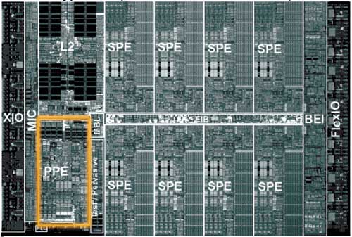
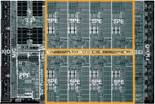
The Cell architecture debuted in a configuration of 9 independent cores: one PowerPC Processing Element (PPE) and eight Synergistic Processing Elements (SPEs). The PPE and SPEs are obviously different, but all eight SPEs are identical to one another.The PPE is IBM's major contribution to the Cell project; it also appears to be very similar to the core being used in the next Xbox console.

The PPE features a 64KB L1 cache and a 512KB L2 cache and features SMT, similar to Intel's Hyper Threading. The PPE features a strictly in-order core, which the desktop x86 market hasn't seen since the death of the original Pentium (the Pentium Pro brought out-of-order execution to the x86 market), so the move for an in-order core is an interesting one. The PPE is also only a 2-issue core, meaning that, at best, it can execute two instructions simultaneously. For comparison, the Athlon 64 is a 3-issue core, so immediately, you get the sense that the PPE is a much simpler core than anything that we have on the desktop. IBM's VMX instruction set (aka Altivec) is also supported by the PPE. Much like the rest of the Cell processor, the PPE is designed to run at very high clock speeds.
There's not much that's impressive about the PPE, other than it's a small, fast, efficient core. Put up against a Pentium 4 or an Athlon 64, the PPE would lose undoubtedly, but the PPE's architecture is one answer to a shift in the performance paradigm. Performance in business/office applications requires a very powerful, very fast general purpose microprocessor, but performance in a game console, for example, does not. The original Xbox used a modified Intel Celeron processor running at 733MHz, while the fastest desktops had 2.0GHz Pentium 4s and 1.60GHz Athlon XPs. Given that the first implementation of Cell is supposed to be Sony's Playstation 3, the simplicity of the PPE is not surprising. Should Cell ever make its way into a PC, the PPE would definitely have to be beefed up, or at least paired with multiple other PPEs.
The majority of the Cell's die is composed of the eight Synergistic Processing Elements (SPEs). If you consider the PPE to be a general purpose microprocessor, think of the SPEs as general purpose processors with a slightly more specific focus.

The SPEs have no branch predictor, meaning that they rely solely on software branch prediction. There are ways that the compiler can avoid branches, and the SPE architecture lends itself very well to things like loop unrolling. Any elementary programmer is familiar with a loop, where one or more lines of code is repeated until a certain condition is met. The checking of that condition (e.g. i < 100) often results in a branch, so one way of removing that branch is simply to unroll the loop. If you have a statement in a loop that is supposed to execute 100 times, you could either keep it in the loop and execute it that way, or you could remove the loop and simply copy the statement 100 times. The end result is the same - the only difference is that in one case, you have a branch condition while the other case results in more lines of code to execute.
The problem with loop unrolling is that you need a large number of registers to unroll some loops, which is one reason that each SPE has 128 registers. Originally, the SPEs were supposed to use the VMX (Altivec) ISA, but because of a need for more than 32 architectural registers, the SPEs implemented a new ISA with support for 128 registers.
Each SPE is only capable of issuing two instructions per clock, meaning that at best, each SPE can execute two instructions at the same time. The issue width of a microprocessor can determine a big part of how large the microprocessor will be; for example, the Itanium 2 is a 6-issue core, so being a 2-issue core makes each SPE significantly smaller than most general purpose microprocessors.
In the end, what we see with the SPEs is that they sacrifice some of the normal tricks to improve ILP in favor of being able to cram more SPEs onto a single die, effectively sacrificing some ILP for greater TLP. Given the direction that the industry is headed, a move to a very TLP centric design makes a lot of sense, but at the same time, it will be quite dependent on developers adhering to very specific development models.
Clearly, the architects of Cell saw the SPEs as being used to run a highly parallelizable workload, and as Derek Wilson mentioned in his article about AGEIA's PhysX PPU:
"One of the properties of graphics that made the feature a good fit for a specialized processor inside a PC is the fact that the task is infinitely parallelizable. Hundreds of thousands, and even millions of pixels, need to be processed every frame. The more detailed a rendering needs to be, the more parallel the task becomes. The same is true with physics. As with the visual world, the physical world is continuous rather than discrete. The more processing power we have, the more things we can simulate at once, and the more realistically we can approximate the real world."
With NVIDIA supplying some form of a GPU for Playstation 3, Cell's array of SPEs have one definite purpose in a gaming console - physics and AI processing. Many have argued that the array of SPEs seems capable of taking over the pixel processing workload of a GPU, but for a high performance console, that's not much of an option. The SPE array could offer better CPU-based 3D rendering, but it would be a tough sell (no pun intended) for this array of SPEs to be the end of dedicated GPU hardware.


70 Comments
View All Comments
faboloso112 - Thursday, March 17, 2005 - link
ahh i love bedtime stories!great read...VERY informative!
ksherman - Thursday, March 17, 2005 - link
sweet article! way over my head, but there were some parts that were dropped down to my level of understanding. Leave it to anand to tell the real story. It will be interesting to see how willing some companies will be to accomidate Sony's ratical processor... bu tas long as theirs money... Do you think that it is possible to (down the road) flop a x86 chip in place of the PPE? wouldn't hat make the Cell compatible with the current processing standards?ProviaFan - Thursday, March 17, 2005 - link
Describing this as a "sit down read" type of article makes me want to print it out to put it in the magazine rack, because I don't have a laptop + 802.11g to peruse AnandTech while I'm, er... ;)xsilver - Thursday, March 17, 2005 - link
nice, definitley one of those "sit down reads".... some serious shiznit ;)cosmotic - Thursday, March 17, 2005 - link
OMG! FIRST POST LOL ROFL LMAO OMG!!! LOOK WHOS COOL!!!Fricardo - Thursday, March 17, 2005 - link
Finally! Thanks guys.Bawl - Saturday, January 25, 2014 - link
I just love this deep analysis of one of the most mist-understanding processor of the last decade.Too bad that after spending more than a half-of-billion dollars, SonyThoshibaIBM didn't release the presumably outstanding CellTwo.
Ferrx - Sunday, December 20, 2015 - link
Hi, can you help me to understand this ? I don't understand at all about these._______ _________ ______
|Decode| | Execute | | Write |
----------- ---------------- -----------
| I1 | I2 | | | | | | | |
| I3 | I4 | | I1 | I2 | | | | |
| I3 | I4 | | I1 | | | | I2 | |
| | I4 | | | | | | I1 | I3 |
| I5 | I6 | | | | I4 | | I4 | |
| | I6 | | | I5 | | | I5 | |
| | | | | I6 | | | I6 | |
_______ _________ ______
In "Decode", each row has 2 columns. What do First and Second Column mean ?
same as "Write"
And in "Execute, each row has 3 columns. What do First, Second and Third column mean ?
And how is the process ? (The current table is about "In-Order Issue with Out-of-Order Completion").
I've read it many times, in the "Instruction Level Parallelism". But I still don't have any idea about it.
Ferrx - Sunday, December 20, 2015 - link
Aww... Can't do tab-'ing' 0__0