Asus A8N-VM CSM: NVIDIA GeForce 6150 Finally Arrives
by Wesley Fink on December 1, 2005 12:04 AM EST- Posted in
- Motherboards
More Features: Asus A8N-VM CSM
The 4 DIMMs support up to 4GB of ECC/non-ECC unregistered DDR memory in a dual-channel configuration. The color coding is correct here - match colors for each channel - but this places the DIMMs with no spacing in-between in a 2-dimm setup. IDE and Floppy cable connections are all at the upper right edge, which is normally the best location.
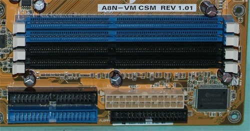
The 4 DIMMs support up to 4GB of ECC/non-ECC unregistered DDR memory in a dual-channel configuration. The color coding is correct here - match colors for each channel - but this places the DIMMs with no spacing in-between in a 2-dimm setup. IDE and Floppy cable connections are all at the upper right edge, which is normally the best location.



56 Comments
View All Comments
highlandsun - Thursday, December 1, 2005 - link
Yes, Googer is missing the point that this is supposed to be a complete *Media Center*, that means audio too. I need SPDIF in/out for my minidiscs and other audio devices. I have a multichannel amplifier but I'd prefer to feed it with a pure digital signal. And yes, the PCI slots are already spoken for (Fusion HDTV tuner).BigLan - Thursday, December 1, 2005 - link
Actually, spdif and HD audio are pretty much mutually exclusive. The main benefit of spdif is to pass a dolby digital or dts audio stream untouched to a receiver from the dvd disk (or .avi file.) HD audio allows the motherboard to do 7.1 sound on the motherboard, which is then sent out of the analogue outputs - the 7.1 sound in games etc doesn't use spdif unless you have a soundstorm2 board or certain soundcards which do dolby digital encoding.For most HTPCs, HD audio doesn't actually do anything.
Googer - Thursday, December 1, 2005 - link
If i am not mistaken, ATI's chipset allows for 32 or 64MB of dedicated video RAM to be soldered in to the motherboard. This prevents it from having to resort to system memory.USAF1 - Thursday, December 1, 2005 - link
Hmm... I could be mistaken, but I'm pretty sure that the Marvell 88E1111 "Alaska" chip is just functioning as the PHY for the GbE resident in the nForce 430 southbridge chip. I don't see anything in the 88E1111 tech docs that indicate that it's a fully functional PCIe GbE controller - for that you'd need something like the Marvell's 88E8050 "Yukon" chip. Here are some links:http://www.marvell.com/products/transceivers/singl...">http://www.marvell.com/products/transceivers/singl...
http://www.marvell.com/products/transceivers/singl...">http://www.marvell.com/products/transce.../Alaska_...'marvell%2088e1111'
http://www.marvell.com/products/pcconn/yukon/index...">http://www.marvell.com/products/pcconn/yukon/index...
Wesley Fink - Thursday, December 1, 2005 - link
The Marvell is a Gigabit PHY, just as in other nForce4 chipsets. As our benchmarks show, it is definitely operating at PCIe speeds.USAF1 - Thursday, December 1, 2005 - link
The fact that a certain PHY (Marvell 88E1111, Vitesse VSC8201RX, etc) and nForce4 MAC combo runs at speeds similar to a dedicated PCIe controller, doesn't make it a PCIe-based solution. Your article would lead one to believe that the Marvell 88E1111 is a PCIe-enabled GbE controller, which in fact it is not.Wesley Fink - Thursday, December 1, 2005 - link
We stated clearly in the Features Chart that the Marvel is a PHY (Physical Layer) chip. This is what we have been seeing in nF4 chipsets for quite a while.USAF1 - Thursday, December 1, 2005 - link
Sorry Wesley, but I still think that your article is misleading. The quote "Asus used the PCIe Gigabit hooks in the 430 Southbridge to provide PCIe Gigabit LAN on the A8N-VM." is just not factual. Neither are the "PCIe" labels next to "Marvell 88E1111" on your graphs. The fact of the matter is that there is no PCIe GbE on this board, yet it's plastered all over the "ethernet performance" section of your article. Why don't you just fix the mistake? Where is Anandtech's vaunted journalistic integrity???Wesley Fink - Friday, December 2, 2005 - link
Upon further research, it does look like the 88E1111 does use a different approach to Gigabit LAN than the PCIe solutions. Marvell refers to the chip as a "Single Port Transceiver". From a users perspective, the performance was found to be the same as PCIe Ethernet, but we have made a few changes in the wording and graphs to more accurately describe the Gigabit LAN used on this board.USAF1 - Friday, December 2, 2005 - link
Thank you very much, Wesley. Now I can stop talking bad about you and your extended family. ;)