NVIDIA's Tiny 90nm G71 and G73: GeForce 7900 and 7600 Debut
by Derek Wilson on March 9, 2006 10:00 AM EST- Posted in
- GPUs
NVIDIA's Die Shrink: The 7900 and 7600
The first major benefit to NVIDIA comes in the form of die size. The original G70 is a 334mm^2 chip, while the new 90nm GPUs are 196mm^2 and 125mm^2 for G71 and G73 respectively. Compare this to the G72 (the chip used in the 7300) at 77mm^2 and the R580 at 353mm^2 for a good idea of the current range in sizes for 90nm GPUs and you will see that NVIDIA hardware is much smaller than ATI hardware in general. The reasons behind the difference in die size between the high end ATI and NVIDIA hardware comes down to the design decisions made by ATI and NVIDIA. ATI decided to employ full-time fp32 processing with very good loop granularity, floating point blend with anti-aliasing, a high quality anisotropic filtering option, and the capability to support more live registers at full speed in a shader program. These are certainly desirable features, but NVIDIA has flat out told us that they don't believe most of these features have a place in hardware based on current and near term games and the poor performance characteristics of code that makes use of them.
Of course, in graphics there are always chicken and egg problems. We would prefer it if all companies could offer all features at high performance for a low cost, but this just isn't possible. We applaud ATI's decision to stick their neck out and include some truly terrific features at the expense of die size, and we hope it inspires some developers out there to really take advantage of what SM3.0 has to offer. At the same time, a hardware feature that goes unused is useless (hardware is only as good as the software it runs allows it to be). If NVIDIA is right about the gaming landscape, a smaller die size with great performance in current and near term games does give NVIDIA a clear competitive edge. Also note that NVIDIA has been an early adopter of features in the past that went largely unused (i.e. fp32 in the FX line), so perhaps they've learned from past experience.
The smaller the die, the more chips can fit on one silicon wafer. As the wafer costs the same to manufacture regardless of the number of ICs or yield, having a small IC and high yield decrease the cost per die to NVIDIA. Lower cost per die is a huge deal in the IC industry, especially in the GPU segment. Not only does a lower cost to NVIDIA mean the opportunity for higher profit margins, it also gives them the ability to be very aggressive with pricing while still running in the black. With ATI's newest lineup offering quite a bit of performance and more features than NVIDIA hardware, this is all good news for consumers. ATI has a history of being able to pull out some pretty major victories when they need to, but with NVIDIA's increased flexibility we hope to see more bang for your buck across the board.
We haven't had the opportunity to test an X1800 GTO for this launch. We requested a board from ATI, but they were apparently unable to ship us one before the launch. The ability of ATI to sustain this product as well as it did the X800 GTO is certainly questionable as well (after all, the X800 GTO could be built from any of three different GPUs from different generations while the X1800 GTO has significantly fewer options). However, we are hopeful that the X1800 GTO will be a major price performance leader that will put pressure on NVIDIA to drop the price of their newest parts even lower than they already are. After all, in the end we are our readers' advocates: we want to see what is best for our community, and a successful X1800 GTO and the flexibility of NVIDIA after this die shrink would certainly be advantageous for all enthusiasts. But we digress.
The end result of this die shrink, regardless of where the prices on these parts begin to settle, is two new series in the GeForce line: the 7900 at the high end and 7600 at the midrange.
The Newest in High End Fashion
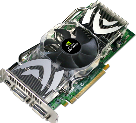
The GeForce 7900 Series is targeted squarely at the top. The 7900 GTX assumes its position at the top of the top, while the 7900 GT specs out very similarly to the original 7800 GTX. Due to the 90nm design, NVIDIA was able to target power and thermal specifications similar to the 7800 GTX 512 with the new 7900 GTX and get much higher performance. In the case of the 7900 GT, performance levels on the order of the 7800 GTX can be delivered in a much smaller, cooler package that pulls less power.
While the 7900 GTX will perform beyond anything else NVIDIA has on the table now, the 7900 GT should give NVIDIA a way to provide a more cost effective and efficient solution to those who wish to achieve 7800 GTX level performance. The specifics of the new lineup are as follows:
7900 GTX:
8 vertex pipes
24 pixel pipes
16 ROPs
650 MHz core clock
1600 MHz memory data rate
512MB of memory on a 256bit bus
$500 +
7900 GT:
8 vertex pipes
24 pixel pipes
16 ROPs
450 MHz core clock
1320 MHz memory data rate
256MB of memory on a 256bit bus
$300 - $350
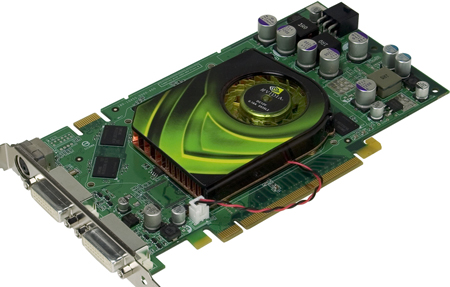
Image wise, the 7900 GTX takes on the same look as the 7800 GTX 512 with its massive heatsink and large PCB. In sharp contrast to the more powerful 7900 and its 110nm brother, the 7800 GTX 512MB, the 7900 GT sports a rather lightweight heatsink/fan solution. Take a look at the newest high end cards to step onto the stage:
Midrange Chic
With the introduction of the 7600 GT, NVIDIA is hoping they have an X1600 XT killer on their hands. Not only is this part designed to perform better than a 6800 GS, but NVIDIA is hoping to keep it price competitive with ATI's upper midrange. Did we mention it also requires no external power?
In our conversations with NVIDIA about this launch, they really tried to drive home the efficiency message. They like to claim that their parts have fewer transistors and provide performance similar to or greater than competing ATI GPUs (ignoring the fact that the R5xx GPU actually has more features than the G70 and processes everything at full precision). When sitting in on a PR meeting, it's easy to dismiss such claims as hype and fluff, but seeing the specs and performance of the 7600 GT coupled with its lack of power connector and compact thermal solution opened up our eyes to what efficiency can mean for the end user. This is what you get packed into this sleek midrange part:
7600 GT
5 vertex pipes
12 pixel pipes
8 ROPs
560 MHz core clock
1400 MHz memory data rate
256MB of memory on a 128bit bus
$180 - $230
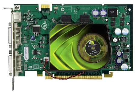
And as NVIDIA wants this card to evolve into the successor to the 6600 GT, we get all of that in a neat little package:
Now that we've taken a look at what NVIDIA is offering this time around, let us take a step back and absorb the competitive landscape.
The first major benefit to NVIDIA comes in the form of die size. The original G70 is a 334mm^2 chip, while the new 90nm GPUs are 196mm^2 and 125mm^2 for G71 and G73 respectively. Compare this to the G72 (the chip used in the 7300) at 77mm^2 and the R580 at 353mm^2 for a good idea of the current range in sizes for 90nm GPUs and you will see that NVIDIA hardware is much smaller than ATI hardware in general. The reasons behind the difference in die size between the high end ATI and NVIDIA hardware comes down to the design decisions made by ATI and NVIDIA. ATI decided to employ full-time fp32 processing with very good loop granularity, floating point blend with anti-aliasing, a high quality anisotropic filtering option, and the capability to support more live registers at full speed in a shader program. These are certainly desirable features, but NVIDIA has flat out told us that they don't believe most of these features have a place in hardware based on current and near term games and the poor performance characteristics of code that makes use of them.
Of course, in graphics there are always chicken and egg problems. We would prefer it if all companies could offer all features at high performance for a low cost, but this just isn't possible. We applaud ATI's decision to stick their neck out and include some truly terrific features at the expense of die size, and we hope it inspires some developers out there to really take advantage of what SM3.0 has to offer. At the same time, a hardware feature that goes unused is useless (hardware is only as good as the software it runs allows it to be). If NVIDIA is right about the gaming landscape, a smaller die size with great performance in current and near term games does give NVIDIA a clear competitive edge. Also note that NVIDIA has been an early adopter of features in the past that went largely unused (i.e. fp32 in the FX line), so perhaps they've learned from past experience.
The smaller the die, the more chips can fit on one silicon wafer. As the wafer costs the same to manufacture regardless of the number of ICs or yield, having a small IC and high yield decrease the cost per die to NVIDIA. Lower cost per die is a huge deal in the IC industry, especially in the GPU segment. Not only does a lower cost to NVIDIA mean the opportunity for higher profit margins, it also gives them the ability to be very aggressive with pricing while still running in the black. With ATI's newest lineup offering quite a bit of performance and more features than NVIDIA hardware, this is all good news for consumers. ATI has a history of being able to pull out some pretty major victories when they need to, but with NVIDIA's increased flexibility we hope to see more bang for your buck across the board.
We haven't had the opportunity to test an X1800 GTO for this launch. We requested a board from ATI, but they were apparently unable to ship us one before the launch. The ability of ATI to sustain this product as well as it did the X800 GTO is certainly questionable as well (after all, the X800 GTO could be built from any of three different GPUs from different generations while the X1800 GTO has significantly fewer options). However, we are hopeful that the X1800 GTO will be a major price performance leader that will put pressure on NVIDIA to drop the price of their newest parts even lower than they already are. After all, in the end we are our readers' advocates: we want to see what is best for our community, and a successful X1800 GTO and the flexibility of NVIDIA after this die shrink would certainly be advantageous for all enthusiasts. But we digress.
The end result of this die shrink, regardless of where the prices on these parts begin to settle, is two new series in the GeForce line: the 7900 at the high end and 7600 at the midrange.
The Newest in High End Fashion
The GeForce 7900 Series is targeted squarely at the top. The 7900 GTX assumes its position at the top of the top, while the 7900 GT specs out very similarly to the original 7800 GTX. Due to the 90nm design, NVIDIA was able to target power and thermal specifications similar to the 7800 GTX 512 with the new 7900 GTX and get much higher performance. In the case of the 7900 GT, performance levels on the order of the 7800 GTX can be delivered in a much smaller, cooler package that pulls less power.
While the 7900 GTX will perform beyond anything else NVIDIA has on the table now, the 7900 GT should give NVIDIA a way to provide a more cost effective and efficient solution to those who wish to achieve 7800 GTX level performance. The specifics of the new lineup are as follows:
7900 GTX:
8 vertex pipes
24 pixel pipes
16 ROPs
650 MHz core clock
1600 MHz memory data rate
512MB of memory on a 256bit bus
$500 +
7900 GT:
8 vertex pipes
24 pixel pipes
16 ROPs
450 MHz core clock
1320 MHz memory data rate
256MB of memory on a 256bit bus
$300 - $350
Image wise, the 7900 GTX takes on the same look as the 7800 GTX 512 with its massive heatsink and large PCB. In sharp contrast to the more powerful 7900 and its 110nm brother, the 7800 GTX 512MB, the 7900 GT sports a rather lightweight heatsink/fan solution. Take a look at the newest high end cards to step onto the stage:


Midrange Chic
With the introduction of the 7600 GT, NVIDIA is hoping they have an X1600 XT killer on their hands. Not only is this part designed to perform better than a 6800 GS, but NVIDIA is hoping to keep it price competitive with ATI's upper midrange. Did we mention it also requires no external power?
In our conversations with NVIDIA about this launch, they really tried to drive home the efficiency message. They like to claim that their parts have fewer transistors and provide performance similar to or greater than competing ATI GPUs (ignoring the fact that the R5xx GPU actually has more features than the G70 and processes everything at full precision). When sitting in on a PR meeting, it's easy to dismiss such claims as hype and fluff, but seeing the specs and performance of the 7600 GT coupled with its lack of power connector and compact thermal solution opened up our eyes to what efficiency can mean for the end user. This is what you get packed into this sleek midrange part:
7600 GT
5 vertex pipes
12 pixel pipes
8 ROPs
560 MHz core clock
1400 MHz memory data rate
256MB of memory on a 128bit bus
$180 - $230
And as NVIDIA wants this card to evolve into the successor to the 6600 GT, we get all of that in a neat little package:

Now that we've taken a look at what NVIDIA is offering this time around, let us take a step back and absorb the competitive landscape.


97 Comments
View All Comments
DigitalFreak - Thursday, March 9, 2006 - link
I saw that as well. Any comments, Derek?DerekWilson - Thursday, March 9, 2006 - link
I did not see any texture shimmering during testing, but I will make sure to look very closely druing our follow up testing.Thanks,
Derek Wilson
jmke - Thursday, March 9, 2006 - link
just dropped by to say that you did a great job here, plenty of info, good benchmarks, nice "load/idle" tests. not many people here know how stresfull benchmarking against the clock can be. keep up the good work. Looking forward to the follow-up!Spinne - Thursday, March 9, 2006 - link
I think it's safe to say that atleast for now, there is no clear winner with a slight advantage to ATI. From the bechmarks, it seems that the 7900GTX performs on par with the X1900XT with the X1900XTX a few fps higher (not a huge diff IMO). The future will therefore be decided by the drivers and the games. The drivers are still pretty young and I bet we'll see performance improvements in the future as both sets of drivers mature. The article says, ATI has the more comprehensive graphics solution (sorta like the R420 vs/s the NV40 situation in reverse?), so if code developers decide to take advantage of the greater functionality offered by ATI (most coders will probably aim for the lowest common denominator to increase sales, while a few may have 'ATI only' type features) then that may tilt the balance in ATI's favor. What's more important is the longevity of the R580 & G71 families. With VISTA set to appear towards the end of the year, how long can ATI and NVIDIA push these DX9 parts? I'm sure both companies will have a new family ready for VISTA, though the new family may just be a more refined version of the R580 and G71 architectures (much as the R420 was based off the R300 family). In terms of raw power, I think we're already VISTA games ready.The real question is, what does DX10 bring to the table from the perspective of the end user? There were certain features unique to DX9 that a DX8 part just could not render. Are there things that a DX10 card will be able to do that a DX9 card just can't do? As I understand it, the main difference between DX9 and 10 is that DX10 will unify Pixel Shaders and Vertex shaders, but I don't see how this will let a DX10 card render something that a DX9 card can't. Can anyone clarify?
Lastly, one great benefit of Crossfire and SLI will be that I can buy a high end X1900XT for gaming right now and then add a low end card or a HD accelerator card (like the MPEG accelerator cards a few yyears ago) when it is clear if HDCP support will be necessary to play HD content and when I can afford to add a HDCP compliant monitor.
yacoub - Friday, March 10, 2006 - link
And price, bro, and price. Two cards at the same performance level from two different companies = great time for a price war. Especially when one has the die shrink advantage as an incentive to drop the price to squeeze out the other's profits.
bob661 - Thursday, March 9, 2006 - link
I only buy based on games I play anyways but it's good to see them close in performance.DerekWilson - Thursday, March 9, 2006 - link
The major difference that DX9 parts will "just not be able to do" is vertex generation and "geometry shading" in hardware. Currently a vertex shader program can only manipulate existing data, while in the future it will be possible to adaptively create or destroy vertecies.Programmatically, the transition from DX9 to DX10 will be one of the largest we have seen in a while. Or so we have been told. Some form of the DX10 SDK (not sure if it was a beta or not) was recently released, so I may look into that for more details if people are interested.
feraltoad - Friday, March 10, 2006 - link
I too would be very interested to learn more about DX10. I have looked online but I haven't really seen anything beyond the unification u mentioned.Also Unreal 2007 does look ungodly, and I didn't even think to wonder if it was DX9 or 10 like the other poster. Will it be comparable to games that will run on 8.1 hardware sans DX9 effects? That engine will make them big bux when they license it out. Sidenote-I read they were running demos of it with a quad SLI setup to showcase the game. I wonder what it will need to run it at full tilt?
BTW Derek I think you do a very good job at AT, I always find your articles full of good common sense advice. When U did a review on the 3000+ budget gaming platform I jumped on the A64 bandwagon (I had to get an AsrockDual tho, instead of an NF4 cuz I wanted to keep my AGP 6600gt, and that's sad now considering the 7900 gt performance/price in sli compared to a 7900gtx.) and I've been really happy with my 3000+ at 2250 it runs noticeably better than my XP2400M oc'd 2.2) I'm just one example of someone you & AT have made more satisfied with their PC experience. So don't let disparaging comments get you down. You thorough committment to accuracy of your work shows how you accept criticism with grace and correct mistakes swiftly. I think the only thing "slipping" around here are peoples' manners.
Spinne - Thursday, March 9, 2006 - link
Yes, please do! So if you can actually generate vertices, the impact would be that you'd be able to do stuff like the character's hair flying apart in a light breeze without having to create the hair as a high poly model, right? What about the Unreal3 engine? Is it a DX9 or DX10 engine?Rock Hydra - Thursday, March 9, 2006 - link
I didn't read all of that, but I'm glad it's close becasue the consumer becomes the real winner.