Intel's Core 2 Extreme & Core 2 Duo: The Empire Strikes Back
by Anand Lal Shimpi on July 14, 2006 12:00 AM EST- Posted in
- CPUs
The architecture is called Core, processor family is Core 2, the product names are Core 2 Duo and Core 2 Extreme. In the past we've talked about its architecture and even previewed its performance, but today is the real deal. We've all been waiting for this day, the day Intel lifts the last remaining curtain on the chip that is designed to re-take the performance crown from AMD, to return Intel to its days of glory.
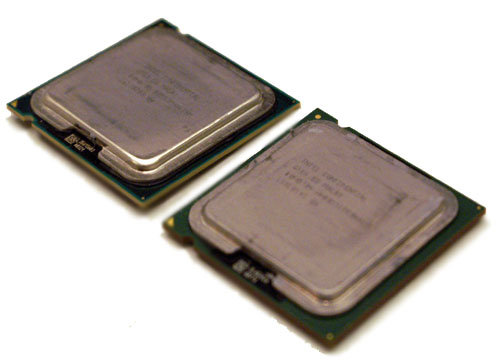
It sure looks innocent enough:

Core 2 Duo (left) vs. Pentium D (right)
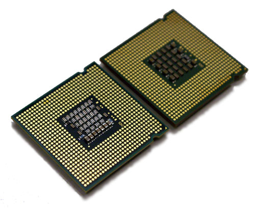
What you see above appears to be no different than a Pentium D. Honestly, unless you flip it over there's no indication of what lies beneath that dull aluminum heat spreader.

Core 2 Duo (left) vs. Pentium D (right)
But make no mistake, what you see before you is not the power hungry, poor performing, non-competitive garbage (sorry guys, it's the truth) that Intel has been shoving down our throats for the greater part of the past 5 years. No, you're instead looking at the most impressive piece of silicon the world has ever seen - and the fastest desktop processor we've ever tested. What you're looking at is Conroe and today is its birthday.
Intel's Core 2 launch lineup is fairly well rounded as you can see from the table below:
| CPU | Clock Speed | L2 Cache |
| Intel Core 2 Extreme X6800 | 2.93GHz | 4MB |
| Intel Core 2 Duo E6700 | 2.66GHz | 4MB |
| Intel Core 2 Duo E6600 | 2.40GHz | 4MB |
| Intel Core 2 Duo E6400 | 2.13GHz | 2MB |
| Intel Core 2 Duo E6300 | 1.86GHz | 2MB |
As the name implies, all Core 2 Duo CPUs are dual core as is the Core 2 Extreme. Hyper Threading is not supported on any Core 2 CPU currently on Intel's roadmaps, although a similar feature may eventually make its debut in later CPUs. All of the CPUs launching today also support Intel's Virtualization Technology (VT), run on a 1066MHz FSB and are built using 65nm transistors.
The table above features all of the Core 2 processors Intel will be releasing this year. In early next year Intel will also introduce the E4200, which will be a 1.60GHz part with only a 800MHz FSB, a 2MB cache and no VT support. The E4200 will remain a dual core part, as single core Core 2 processors won't debut until late next year. On the opposite end of the spectrum Intel will also introduce Kentsfield in Q1 next year, which will be a Core 2 Extreme branded quad core CPU from Intel.
Core 2 Extreme vs. Core 2 Duo
 Previously Intel had differentiated its "Extreme" line of processors by giving them larger caches, a faster FSB, Hyper Threading support, and/or higher clock speeds. With the Core 2 processor family, the Extreme version gets a higher clock speed (2.93GHz vs. 2.66GHz) and this time around it also gets an unlocked multiplier. Intel officially describes this feature as the following:
Core 2 Extreme is not truly "unlocked". Officially (per the BIOS Writers Guide), it is "a frequency limited processor with additional support for ratio overrides higher than the maximum Intel-tested bus-to-core ratio." Currently, that max tested ratio is 11:1 (aka 2.93G @ 1066 FSB). The min ratio is 6:1. However, do note that the Core 2 Extreme will boot at 2.93G unlike prior generation XE processors which booted to the lowest possible ratio and had to be "cranked up" to the performance ratio.
In other words, you can adjust the clock multiplier higher or lower than 11.0x, which hasn't been possible on a retail Intel chip for several years. By shipping the Core 2 Extreme unlocked, Intel has taken yet another page from AMD's Guide to Processor Success. Unfortunately for AMD, this wasn't the only page Intel took.
Manufacturing Comparison
The new Core 2 processors, regardless of L2 cache size, are made up of 291 million transistors on a 143 mm^2 die. This makes the new chips smaller and cheaper to make than Intel's Pentium D 900 series. The new Core 2 processors are also much smaller than the Athlon 64 X2s despite packing more transistors thanks to being built on a 65nm process vs. 90nm for the X2s.
| CPU | Manufacturing Process | Transistor Count | Die Size |
| AMD Athlon 64 X2 (2x512KB) | 90nm | 154M | 183 mm^2 |
| Intel Core 2 | 65nm | 291M | 143 mm^2 |
| Intel Pentium D 900 | 65nm | 376M | 162 mm^2 |
Intel's smaller die and greater number of manufacturing facilities results in greater flexibility with pricing than AMD.


202 Comments
View All Comments
coldpower27 - Friday, July 14, 2006 - link
Are there supposed to be there as they aren't functioning in Firefox 1.5.0.4coldpower27 - Friday, July 14, 2006 - link
You guys fixed it awesome.Orbs - Friday, July 14, 2006 - link
On "The Test" page (I think page 2), you write:please look back at the following articles:
But then there are no links to the articles.
Anyway, Anand, great report! Very detailed with tons of benchmarks using a very interesting gaming configuration, and this review was the second one I read (so it was up pretty quickly). Thanks for not saccrificing quality just to get it online first, and again, great article.
Makes me want a Conroe!
Calin - Friday, July 14, 2006 - link
Great article, and thanks for a well done job. Conroe is everything Intel marketing machine shown it to be.stepz - Friday, July 14, 2006 - link
The Core 2 doesn't have smaller emoty latency than K8. You're seeing the new advanced prefetcher in action. But don't just believe me, check with the SM2.0 author.Anand Lal Shimpi - Friday, July 14, 2006 - link
That's what Intel's explanation implied as well, when they are working well the prefetchers remove the need for an on-die memory controller so long as you have an unsaturated FSB. Inevitably there will be cases where AMD is still faster (from a pure latency perspective), but it's tough to say how frequently that will happen.Take care,
Anand
stepz - Friday, July 14, 2006 - link
Excuse me. You state "Intel's Core 2 processors now offer even quicker memory access than AMD's Athlon 64 X2, without resorting to an on-die memory controller.". That is COMPLETELY wrong and misleading. (see: http://www.aceshardware.com/forums/read_post.jsp?i...">http://www.aceshardware.com/forums/read_post.jsp?i... )It would be really nice from journalistic integrity point of view and all that, if you posted a correction or atleast silently changed the article to not be spreading incorrect information.
Oh... and you really should have smelt something fishy when a memory controller suddenly halves its latency by changing the requestor.
stepz - Friday, July 14, 2006 - link
To clarify. Yes the prefetching and espescially the speculative memory op reordering does wonders for realworld performance. But then let the real-world performance results speak for themselves. But please don't use broken synthetic tests. The advancements help to hide latency from applications that do real work. They don't reduce the actual latency of memory ops that that test was supposed to test. Given that the prefetcher figures out the access pattern of the latency test, the test is utterly meaningless in any context. The test doesn't do anything close to realworld, so if its main purpose is broken, it is utterly useless.JarredWalton - Friday, July 14, 2006 - link
Modified comments from a similar thread further down:Given that the prefetcher figures out the access pattern of the latency test, the test is utterly meaningless in any context."
That's only true if the prefetcher can't figure out access patterns for all other applications as well, and from the results I'm pretty sure it can. You have to remember, even with the memory latency of approximately 35 ns, that delay means the CPU now has about 100 cycles to go and find other stuff to do. At an instruction fetch rate of 4 instructions per cycle, that's a lot of untapped power. So, while it waits on main memory access one, it can be scanning the next accesses that are likely to take place and start queuing them up and priming the RAM. The net result is that you may never actually be able to measure latency higher than 35-40 ns or whatever.
The way I think of it is this: pipeline issues aside, a large portion of what allowed Athlon 64 to outperform NetBurst was reduced memory latency. Remember, Pentium 4 was easily able to outperform Athlon XP in the majority of benchmarks -- it just did so at higher clock speeds. (Don't *even* try to tell me that the Athlon XP 3200+ was as fast as a Pentium 4 3.2 GHz! LOL. The Athlon 64 3200+ on the other hand....) AMD boosted performance by about 25% by adding an integrated memory controller. Now Intel is faster at similar clock speeds, and although the 4-wide architectural design helps, not to mention 4MB shared L2, they almost certainly wouldn't be able to improve performance without improving memory latency -- not just in theory, but in actual practice. Looking at the benchmarks, I have to think that our memory latency scores are generally representative of what applications see.
If you have to engineer a synthetic application specifically to fool the advanced prefetcher and op reordering, what's the point? To demonstrate a "worst case" scenario that doesn't actually occur in practical use? In the end, memory latency is only one part of CPU/platform design. The Athlon FX-62 is 61.6% faster than the Pentium XE 965 in terms of latency, but that doesn't translate into a real world performance difference of anywhere near 60%. The X6800 is 19.3% faster in memory latency tests, and it comes out 10-35% faster in real world benchmarks, so again there's not an exact correlation. Latency is important to look at, but so is memory bandwidth and the rest of the architecture.
The proof is in the pudding, and right now the Core 2 pudding tastes very good. Nice design, Intel.
coldpower27 - Friday, July 14, 2006 - link
But why are you posting the Manchester core's die size?What about the Socket AM2 Windsor 2x512KB model which has a die size of 183mm2?