NVIDIA 680i: The Best Core 2 Chipset?
by Gary Key & Wesley Fink on November 8, 2006 4:45 AM EST- Posted in
- CPUs
nForce 680i Overclocking
The defining area for the 680i chipset has to be overclocking. The 500 family chipsets for Intel performed fine in many areas, but they were one of the worst chipsets available for Intel in overclocking, topping out somewhere below 350 MHz on the bus speeds. This area kept many Enthusiasts from embracing the NVIDIA SLI solution for their Core 2 processors. It appeared NVIDIA had designed the 500 chipset family for spectacular overclocking on the 200 MHz HTT AMD AM2 chipset. The problem, of course, is that Core 2 processors were released at 1067 FSB (266 base bus speed), and the 500 family chipsets did not have anywhere close to the headroom of the competing Intel chipsets.
All of that has changed, NVIDIA tells us, with a 680i that can do 1333 FSB and more and DDR2 memory speeds of 1200 and beyond. To test NVIDIA's claims we tested the EVGA 680i SLI using the following setup:
The overclock results are not a mistake. We managed to reach right at 4.0GHz with an X6800 at 1.575V. This represented the standard 11x ratio at a 1452 FSB. Even more spectacular was the reduced multiplier overclocking, where we reached a 2100 FSB (525 base) at a 7X multiplier AT DEFAULT VOLTAGE.
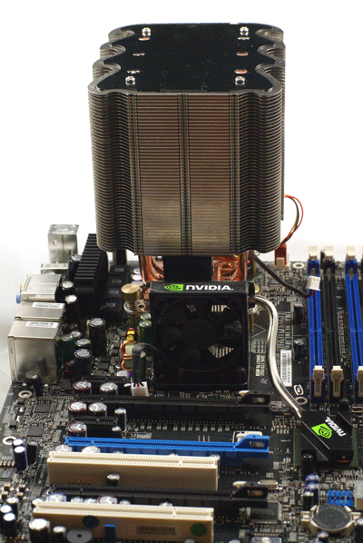
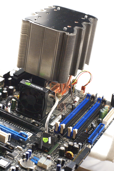
These results were with air cooling using a Tuniq 120 air cooler, which sandwiches a 120mm fan in a finned heatpipe core as pictured above.
One of our X6800 processors reached 2100 FSB, confirming NVIDIA's claims of overclocking an X6800 in their labs to 2070 FSB. Not only did we reach 2100 FSB (525) at a 7X multiplier (3.675GHz), we managed to reach that speed at default voltage. The system has run at those settings for several days without incident and has handled every test and benchmark we have thrown at the system. However, it should also be pointed out that a second X6800 CPU would not overclock 1 MHz higher than 1900 FSB (450) on this same motherboard, even though that X6800 reached a similar 4GHz maximum overclock and similar "default voltage" overclocks.
We have yet to find anything obvious that would explain these differences in maximum FSB in the X6800 chips we tested. Revision and Stepping explained nothing, and we also had four retail E6600 we tested that would not reach above 1800 FSB. We are looking into these findings further and hope to find some explanations to share with you that will explain these maximum FSB differences among 4MB Cache Core 2 chips.
Interestingly, all of the 2MB cache Core 2 processors we tested reached at least 2000 FSB, with the two tested E6300 reaching 2100 FSB (522x7 and 6x525). We were prepared to call the amount of cache the defining difference in FSB performance until the late X6800 reached 2100 in our labs and NVIDIA confirmed their own 2070 results with an X6800 Extreme. We are much more confident that 2MB Cache chips can top 2000 FSB and we are very anxious to find something that will help you identify 4MB cache chips that will reach the "magic" 2000, 2070, and 2100 FSB overclocks.
Overall overclocking performance with the 680i was spectacular, and the results should excite any of you who want to do some serious overclocking with a Core 2 processor. At the very least the nForce 600i chipset family gives shoppers new choices in motherboards that will make the most of their Core 2 processor.
The defining area for the 680i chipset has to be overclocking. The 500 family chipsets for Intel performed fine in many areas, but they were one of the worst chipsets available for Intel in overclocking, topping out somewhere below 350 MHz on the bus speeds. This area kept many Enthusiasts from embracing the NVIDIA SLI solution for their Core 2 processors. It appeared NVIDIA had designed the 500 chipset family for spectacular overclocking on the 200 MHz HTT AMD AM2 chipset. The problem, of course, is that Core 2 processors were released at 1067 FSB (266 base bus speed), and the 500 family chipsets did not have anywhere close to the headroom of the competing Intel chipsets.
All of that has changed, NVIDIA tells us, with a 680i that can do 1333 FSB and more and DDR2 memory speeds of 1200 and beyond. To test NVIDIA's claims we tested the EVGA 680i SLI using the following setup:
| EVGA 680i SLI Overclocking Testbed |
|
| Processor: | Intel Core 2 Extreme X6800 Dual Core, 2.93GHz, 4MB Unified Cache 1066FSB, 11x Multiplier |
| CPU Voltage: | Default (Auto) to 1.575V |
| Cooling: | Tuniq Tower 120 Air Cooling |
| Power Supply: | OCZ GameXstream 700W |
| Memory: | Corsair Dominator 1142MHz (2x1GB) (Micron Memory Chips) |
| Hard Drive | Hitachi 250GB 7200RPM SATA2 16MB Cache |
| Maximum OC: (Standard Ratio) |
363 (1452 FSB) x 11 - 3.993GHz at 1.575V (+36.3%) 334 (1336 FSB) x 11 - 3.675GHz at Default Voltage |
| Maximum OC: (Reduced Multiplier) |
525 (2100 FSB) x 7 - 3.675GHz at Default Voltage |
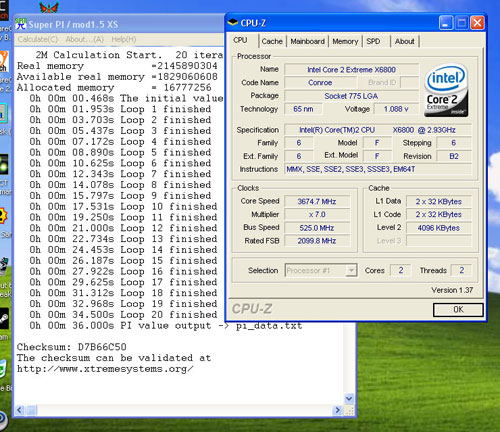
The overclock results are not a mistake. We managed to reach right at 4.0GHz with an X6800 at 1.575V. This represented the standard 11x ratio at a 1452 FSB. Even more spectacular was the reduced multiplier overclocking, where we reached a 2100 FSB (525 base) at a 7X multiplier AT DEFAULT VOLTAGE.


These results were with air cooling using a Tuniq 120 air cooler, which sandwiches a 120mm fan in a finned heatpipe core as pictured above.
 |
| Click to enlarge |
One of our X6800 processors reached 2100 FSB, confirming NVIDIA's claims of overclocking an X6800 in their labs to 2070 FSB. Not only did we reach 2100 FSB (525) at a 7X multiplier (3.675GHz), we managed to reach that speed at default voltage. The system has run at those settings for several days without incident and has handled every test and benchmark we have thrown at the system. However, it should also be pointed out that a second X6800 CPU would not overclock 1 MHz higher than 1900 FSB (450) on this same motherboard, even though that X6800 reached a similar 4GHz maximum overclock and similar "default voltage" overclocks.
We have yet to find anything obvious that would explain these differences in maximum FSB in the X6800 chips we tested. Revision and Stepping explained nothing, and we also had four retail E6600 we tested that would not reach above 1800 FSB. We are looking into these findings further and hope to find some explanations to share with you that will explain these maximum FSB differences among 4MB Cache Core 2 chips.
 |
| Click to enlarge |
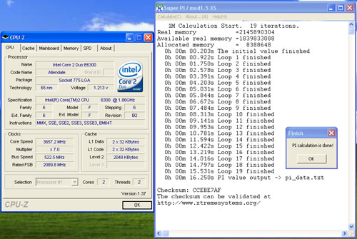
Interestingly, all of the 2MB cache Core 2 processors we tested reached at least 2000 FSB, with the two tested E6300 reaching 2100 FSB (522x7 and 6x525). We were prepared to call the amount of cache the defining difference in FSB performance until the late X6800 reached 2100 in our labs and NVIDIA confirmed their own 2070 results with an X6800 Extreme. We are much more confident that 2MB Cache chips can top 2000 FSB and we are very anxious to find something that will help you identify 4MB cache chips that will reach the "magic" 2000, 2070, and 2100 FSB overclocks.
Overall overclocking performance with the 680i was spectacular, and the results should excite any of you who want to do some serious overclocking with a Core 2 processor. At the very least the nForce 600i chipset family gives shoppers new choices in motherboards that will make the most of their Core 2 processor.


60 Comments
View All Comments
StriderGT - Thursday, November 9, 2006 - link
Also, some Intel chipset fans believe that Intel chipsets are best for a rock solid system (for the record, I'm not one of these people), I guess we'll see if nVidia will change thier minds.No it won't, its the same group of people that suggested the P4 was a more "stable" platform than the Athlon 64 platform. Its simply a psychological state of denial, when someone has paid more for less needs an excuse: "Stability"
skrewler2 - Wednesday, November 8, 2006 - link
I agree with you on your two points.I also wish PM tech was standardized.. I just went through a headache researching what was compatible with what chipset etc, imo it should just all work. From what I understand, the SATA II standard isn't even really a standard at all.. anyways I agree that NV should start implementing Port Multiplier support!
yyrkoon - Wednesday, November 8, 2006 - link
Yeah, I recently bought a budget Asrock board that SUPPOSEDLY supported SATAII connections. As per the standard, SATAII is supposed to support native command queuing (NCQ), and up to 3Gbit/s throughput on each connector. Anyhow this motherboard does not support NCQ . . . which is the majority of the reason to own a SATAII drive / interface, the rest is basicly marketing hype.Kougar - Wednesday, November 8, 2006 - link
Wanted to point out all the tables on the Memory Performance page are mislabled as "980i".Also some power consumption figures would be good, even if not critical. With a chipset cooler that huge it's about a giveaway it is hiding a nice and crispy chipset! ;) Thanks for the article!
Wesley Fink - Wednesday, November 8, 2006 - link
The perils of Table cut-and-paste are now corrected.Please see comments above above Power Consumption. That information will be added to the review since several have requested it.
Avalon - Wednesday, November 8, 2006 - link
I was much more interested in the 650i Ultra boards, specifically how well they overclocked compared to the 680i you benched. Additionally, do you think it's necessary for an active fan cooling the northbridge when highly overclocked on this chipset, or does it run fairly cool?Gary Key - Wednesday, November 8, 2006 - link
We will not have 650i boards until early December for review. The fan is required for upper-end 24/7 overclocking in my opinion, otherwise the board ran fine without it.yzkbug - Wednesday, November 8, 2006 - link
tables in page 10: NVIDIA 980i -> NVIDIA 680iShoNuff - Wednesday, November 8, 2006 - link
I'm impressed with the review. It was very thorough. In particular, I was amazed at your overclock with the X6800. I am looking forward to getting one of these boards in my hands.
It appears that NVIDIA has done it this time with respect to the on board memory controller. It is hard to imagine things getting better when the OEM's add their nuances to this board. If results are this good based upon the reference design, it is almost scary thinking about how good a board DFI would/could produce.
Oh…and btw…I like the new location of the front panel connectors. The new location will make it easier to "stealth" the wires.
hubajube - Wednesday, November 8, 2006 - link
These are ass-kicking OC's!!! Can't wait to own this board.