More Mainstream DX10: AMD's 2400 and 2600 Series
by Derek Wilson on June 28, 2007 8:35 AM EST- Posted in
- GPUs
A Closer Look at RV610 and RV630
The RV6xx parts are similar to the R600 hardware we've already covered in detail. There are a few major differences between the two classes of hardware. First and foremost, the RV6xx GPUs include full video decode acceleration for MPEG-2, VC-1, and H.264 encoded content through AMD's UVD hardware. There was some confusion over this when R600 first launched, but AMD has since confirmed that UVD hardware is not at all present in their high end part.
We also have a difference in manufacturing process. R600 uses an 80nm TSMC process aimed at high speed transistors, while their RV610 and RV630 GPU based cards are fabbed on a 65nm TSMC process aimed at lower power consumption. The end result is that these GPUs will run much cooler and require much less power than their big brother the R600.
Transistor speed between these two processes ends up being similar in spite of the focus on power over performance at 65nm. RV610 is built with 180M transistors, while RV630 contains 390M. This is certainly down from the huge transistor count of R600, but nearly 400M is nothing to sneeze at.
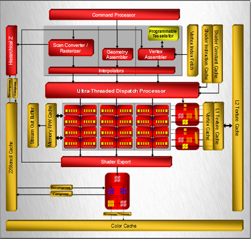
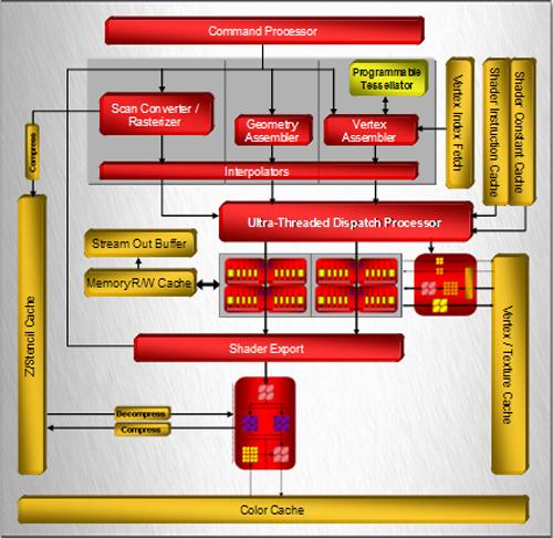
Aside from the obvious differences of transistor count and the number of different units (shaders, texture unit, etc.), the only other major difference is in memory bus width. All RV610 GPU based hardware will have a 64-bit memory bus, while RV630 based parts will feature a 128-bit connection to memory. Here's the layout of each GPU:

RV630 Block Diagram

RV610 Block Diagram
One of the first things that jump out is that both RV6xx based designs feature only one render back end block. This part of the chip is responsible for alpha (transparency) and fog, dealing with final z/stencil buffer operations, sending MSAA samples back up to the shader to be resolved, and ultimately blending fragments and writing out final pixel color. Maximum pixel fill rate is limited by the number of render back ends.
In the case of both current RV6xx GPUs, we can only draw out a maximum of 4 pixels per clock (or we can do 8 z/stencil-only ops per clock). While we don't expect extreme resolutions to be run on these parts (at least not in games), we could run into issues with effects that make heavy use of MRTs (multiple render targets), z/stencil buffers, and antialiasing. With the move to DX10, we expect developers to make use of the additional MRTs they have available, and lower resolutions benefit from AA more than high resolutions as well. We would really like to see higher pixel draw power here. Our performance tests will reflect the fact that AA is not kind to AMD's new parts, because of the lack of hardware resolve as well as the use of only one render back end.
Among the notable features that we will see here are tessellation, which could have an even larger impact on low end hardware for enabling detailed and realistic geometry, and CFAA filtering options. Unfortunately, we might not see that much initial use made of the tessellation hardware, and with the reduced pixel draw and shading power of the RVxx series, we are a little skeptical of the benefits of CFAA.
From here, lets move on and take a look at what we actually get in retail products.
The RV6xx parts are similar to the R600 hardware we've already covered in detail. There are a few major differences between the two classes of hardware. First and foremost, the RV6xx GPUs include full video decode acceleration for MPEG-2, VC-1, and H.264 encoded content through AMD's UVD hardware. There was some confusion over this when R600 first launched, but AMD has since confirmed that UVD hardware is not at all present in their high end part.
We also have a difference in manufacturing process. R600 uses an 80nm TSMC process aimed at high speed transistors, while their RV610 and RV630 GPU based cards are fabbed on a 65nm TSMC process aimed at lower power consumption. The end result is that these GPUs will run much cooler and require much less power than their big brother the R600.
Transistor speed between these two processes ends up being similar in spite of the focus on power over performance at 65nm. RV610 is built with 180M transistors, while RV630 contains 390M. This is certainly down from the huge transistor count of R600, but nearly 400M is nothing to sneeze at.
Aside from the obvious differences of transistor count and the number of different units (shaders, texture unit, etc.), the only other major difference is in memory bus width. All RV610 GPU based hardware will have a 64-bit memory bus, while RV630 based parts will feature a 128-bit connection to memory. Here's the layout of each GPU:


One of the first things that jump out is that both RV6xx based designs feature only one render back end block. This part of the chip is responsible for alpha (transparency) and fog, dealing with final z/stencil buffer operations, sending MSAA samples back up to the shader to be resolved, and ultimately blending fragments and writing out final pixel color. Maximum pixel fill rate is limited by the number of render back ends.
In the case of both current RV6xx GPUs, we can only draw out a maximum of 4 pixels per clock (or we can do 8 z/stencil-only ops per clock). While we don't expect extreme resolutions to be run on these parts (at least not in games), we could run into issues with effects that make heavy use of MRTs (multiple render targets), z/stencil buffers, and antialiasing. With the move to DX10, we expect developers to make use of the additional MRTs they have available, and lower resolutions benefit from AA more than high resolutions as well. We would really like to see higher pixel draw power here. Our performance tests will reflect the fact that AA is not kind to AMD's new parts, because of the lack of hardware resolve as well as the use of only one render back end.
Among the notable features that we will see here are tessellation, which could have an even larger impact on low end hardware for enabling detailed and realistic geometry, and CFAA filtering options. Unfortunately, we might not see that much initial use made of the tessellation hardware, and with the reduced pixel draw and shading power of the RVxx series, we are a little skeptical of the benefits of CFAA.
From here, lets move on and take a look at what we actually get in retail products.


96 Comments
View All Comments
Makaveli - Thursday, June 28, 2007 - link
All of you guys posting wait for the DX 10 benchmarks do u seriously think the FPS is gonna double from DX9. These cards are a joke, and ment for OEM systems. They are not gonna release a good midrange card to creep up on the 2900XT and take sales away from it. And they will make far more money selling these cards to OEM's than the average joe blow. The people who are gonna suffer from this is the fools who buy pc's at Best buy and futureshop, that believe they are getting good gaming cards.All I gotta say is you get what you pay for.
Hugs my X1950Pro 512MB AGP!
guste - Thursday, June 28, 2007 - link
Although Anandtech hasn't posted it yet, it looks as if the lower end 2000-series parts are quite good at HD decode, to the point where CPU utilization goes from 100% to 5%. At least this according to a cumbersome Chinese review I read a week ago.Granted my needs don't apply to practically anyone but the HTPC crowd, but I play games at the native resouloution of my 50" panel, which is 1366x768 and I don't use AA, so the 2600 XT would be nice to pick up, in addition to finally being able to send the output to my receiver. For us in the HTPC community, this card will be a godsend, being quiet and low-power.
I look forward to seeing what Anandtech says about the UVD aspects of thse cards, as that's what I'm interested in.
florrv - Thursday, June 28, 2007 - link
Maybe I completely missed it in the reviews, but can these cards be used in Crossfire mode? That could be one way (albeit very clumsy) way to get you closer to midrange performance for the $200-$250 range...strikeback03 - Friday, June 29, 2007 - link
Just looking at the pictures, it would appear the 2400XT and 2600XT cave the connectors.DavenJ - Thursday, June 28, 2007 - link
Wow. Just wow. I haven't seen so much bashing in a long time. However, through all the nVidia and ATI bashing I'm not surprised that the author left out a very important point. The 2600 XT consumes a mere 45W and the 2400 Pro a mere 25W. That is incredible. There is no need for external power as one might expect on low end parts except I think nVidia has external power on the high end 8600. The ATI cards are made using a 65 nm process which explains the low power consumption.For a less insulting and less bias review, go here
http://www.techpowerup.com/reviews/ATI/HD_2600_XT">http://www.techpowerup.com/reviews/ATI/HD_2600_XT
Have a good day!
DerekWilson - Friday, June 29, 2007 - link
i added power numbers on the test page ...the power performance of the new radeon HD cards is not that great.
coldpower27 - Saturday, June 30, 2007 - link
They are as expected, considering the HD 2600 XT is clocked at 800MHZ with 390 Million Transistors the fact that it consumes equal power as compared to the 289 Million Transistor G84 at 675MHZ I would say for what it's worth the improvements of the 65nm process are showing themselves.coldpower27 - Thursday, June 28, 2007 - link
As you can see from the reviews here the HD 2600 XT and HD 2600 Pro don't consume that much less then the cards from the Nvidia camp.http://www.firingsquad.com/hardware/radeon_hd_2600...">http://www.firingsquad.com/hardware/rad...hd_2600_...
Shintai - Thursday, June 28, 2007 - link
The 8600GTS could easily do without an external power connector. So could a 7900GT for that matter. It´s about the situation in SLI and making sure its a clean supply.DerekWilson - Thursday, June 28, 2007 - link
Who am I biased against? Both NVIDIA and AMD have made terrible mainstream parts.While the 86 GTS does require external power, the 86 GT and lower do not.