Intel's Atom Architecture: The Journey Begins
by Anand Lal Shimpi on April 2, 2008 12:05 AM EST- Posted in
- CPUs
An Unbalanced L1 Cache: We Know Why
The Atom processor is outfitted with fairly large caches, which are quite necessary given its in-order architecture that's very sensitive to high memory latencies. We wrote the following in our initial Atom (Silverthorne) architecture discussion:
"The L1 cache is unusually asymmetric with a 32KB instruction and 24KB data cache, a decision made to optimize for performance, die size, and cost. The L2 cache is an 8-way 512KB design, very similar to what was used in the Core architecture.
While Silverthorne is built entirely on Intel's high-k/metal gate 45nm process, there is one major difference: SRAM cell size. Intel uses a 0.382 um^2 SRAM cell in Silverthorne compared to 0.346 um^2 in Core 2. Each SRAM cell is an 8 transistor design compared to 6 transistors in Core 2. The larger cell size increases the die size of Silverthorne but it draws less power and runs at a lower voltage."
At the time we didn't have a good explanation as to why the Atom's L1 cache wasn't made of equal sized instruction and data caches, which is usually how Intel designs its processors. Since then we have gotten some more insight into the design decision:

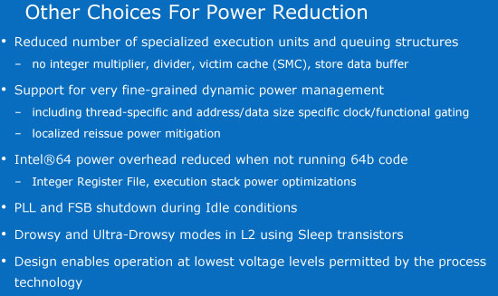
Historically, Intel would design a microprocessor for a particular manufacturing process (e.g. 65nm) and shoot for a target voltage, later attempting to lower that voltage when possible. Atom was designed around the absolute minimum voltage the manufacturing process (45nm) was capable of running at and the engineers were left with the task of figuring out what they could do, architecturally, given that requirement.
The perfect example of this approach to design is Atom's L1 instruction and data caches. Originally these two caches were small signal arrays (6 transistors per cell), they were very compact and delivered the performance Intel desired. However during the modeling of the chip Intel noticed that it was a limiter to being able to scale down the operating voltage of the chip.
Instead of bumping up the voltage and sticking with a small signal array, Intel switched to a register file (1 read/1 write port). The cache now had a larger cell size (8 transistors per cell) which increased the area and footprint of the L1 instruction and data caches. The Atom floorplan had issues accommodating the larger sizes so the data cache had to be cut down from 32KB to 24KB in favor of the power benefits. We wondered why Atom had an asymmetrical L1 data and instruction cache (24KB and 32KB respectively, instead of 32KB/32KB) and it turns out that the cause was voltage.
A small signal array design based on a 6T cell has a certain minimum operating voltage, in other words it can retain state until a certain Vmin. In the L2 cache, Intel was able to use a 6T signal array design since it had inline ECC. There were other design decisions at work that prevented Intel from equipping the L1 cache with inline ECC, so the architects needed to go to a larger cell size in order to keep the operating voltage low.
The end result of this sort of a design approach is that the Atom processor is able to operate at its highest performance state (C0) at its minimum operating voltage.
Hardware Prefetchers: So Necessary
Atom features two hardware prefetchers, one that prefetches from the L2 cache into the L1 data cache and one from memory into the L2 cache.
Hardware prefetching is unbelievably important when dealing with an in-order core because as we've mentioned time and time again, not having data available in cache means that the pipelines will stall until that data is available.
The obvious long term solution to the problem of data starvation is to integrate the memory controller on die. With no 45nm MCH design ready by the time the Atom design was complete, Intel has to wait until the second generation Atom (codename: Moorestown) to gain an on-die memory controller.


46 Comments
View All Comments
lopri - Thursday, April 3, 2008 - link
This article is as much propagana-ish as it is technical. Did you read the last page of the article?clnee55 - Friday, April 4, 2008 - link
Since Anand wrote this article. I let him answer your accusationGulWestfale - Wednesday, April 2, 2008 - link
i believe that the graphics core in the chipset is a powerVR gen5 derivative; intel already uses some of their tech in its existing mainboards and wikipedia states that intel has licensed gen5 tech for one of its chipsets, the GMA500 (which is the same as poulsbo?) gen5 is also DX10-capable, which matches the info in your article.http://en.wikipedia.org/wiki/PowerVR#Series_5_.28S...">http://en.wikipedia.org/wiki/PowerVR#Series_5_.28S...
yyrkoon - Wednesday, April 2, 2008 - link
and wikipedia has been known to be wrong . . . a lot lately it seems.My point here *is*, I would probably trust anandtech more than wikipedia now days, as it seems any Joe can put up a 'reference' without citation.
jones377 - Wednesday, April 2, 2008 - link
Following the references link from the Wiki article...http://www.imgtec.com/News/Release/index.asp?NewsI...">http://www.imgtec.com/News/Release/index.asp?NewsI...
Poulsbo uses a PowerVR 3D core
Anand Lal Shimpi - Wednesday, April 2, 2008 - link
Yep, you guys are correct, I wasn't aware that it was public yet :) I've updated the article.Take care,
Anand