NVIDIA's Fermi: Architected for Tesla, 3 Billion Transistors in 2010
by Anand Lal Shimpi on September 30, 2009 12:00 AM EST- Posted in
- GPUs
Architecting Fermi: More Than 2x GT200
NVIDIA keeps referring to Fermi as a brand new architecture, while calling GT200 (and RV870) bigger versions of their predecessors with a few added features. Marginalizing the efforts required to build any multi-billion transistor chip is just silly, to an extent all of these GPUs have been significantly redesigned.
At a high level, Fermi doesn't look much different than a bigger GT200. NVIDIA is committed to its scalar architecture for the foreseeable future. In fact, its one op per clock per core philosophy comes from a basic desire to execute single threaded programs as quickly as possible. Remember, these are compute and graphics chips. NVIDIA sees no benefit in building a 16-wide or 5-wide core as the basis of its architectures, although we may see a bit more flexibility at the core level in the future.
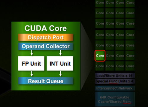
Despite the similarities, large parts of the architecture have evolved. The redesign happened at low as the core level. NVIDIA used to call these SPs (Streaming Processors), now they call them CUDA Cores, I’m going to call them cores.

All of the processing done at the core level is now to IEEE spec. That’s IEEE-754 2008 for floating point math (same as RV870/5870) and full 32-bit for integers. In the past 32-bit integer multiplies had to be emulated, the hardware could only do 24-bit integer muls. That silliness is now gone. Fused Multiply Add is also included. The goal was to avoid doing any cheesy tricks to implement math. Everything should be industry standards compliant and give you the results that you’d expect.
Double precision floating point (FP64) performance is improved tremendously. Peak 64-bit FP execution rate is now 1/2 of 32-bit FP, it used to be 1/8 (AMD's is 1/5). Wow.
NVIDIA isn’t disclosing clock speeds yet, so we don’t know exactly what that rate is yet.
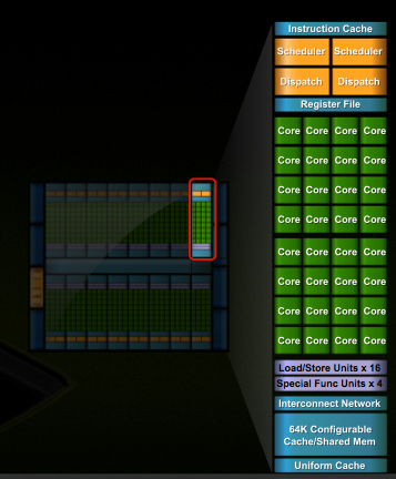
In G80 and GT200 NVIDIA grouped eight cores into what it called an SM. With Fermi, you get 32 cores per SM.

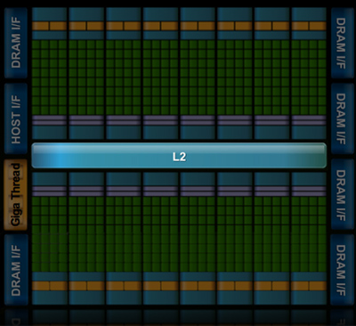
The high end single-GPU Fermi configuration will have 16 SMs. That’s fewer SMs than GT200, but more cores. 512 to be exact. Fermi has more than twice the core count of the GeForce GTX 285.
| Fermi | GT200 | G80 | |
| Cores | 512 | 240 | 128 |
| Memory Interface | 384-bit GDDR5 | 512-bit GDDR3 | 384-bit GDDR3 |
In addition to the cores, each SM has a Special Function Unit (SFU) used for transcendental math and interpolation. In GT200 this SFU had two pipelines, in Fermi it has four. While NVIDIA increased general math horsepower by 4x per SM, SFU resources only doubled.
The infamous missing MUL has been pulled out of the SFU, we shouldn’t have to quote peak single and dual-issue arithmetic rates any longer for NVIDIA GPUs.
NVIDIA organizes these SMs into TPCs, but the exact hierarchy isn’t being disclosed today. With the launch's Tesla focus we also don't know specific on ROPs, texture filtering or anything else related to 3D graphics. Boo.
A Real Cache Hierarchy
Each SM in GT200 had 16KB of shared memory that could be used by all of the cores. This wasn’t a cache, but rather software managed memory. The application would have to knowingly move data in and out of it. The benefit here is predictability, you always know if something is in shared memory because you put it there. The downside is it doesn’t work so well if the application isn’t very predictable.
Branch heavy applications and many of the general purpose compute applications that NVIDIA is going after need a real cache. So with Fermi at 40nm, NVIDIA gave them a real cache.
Attached to each SM is 64KB of configurable memory. It can be partitioned as 16KB/48KB or 48KB/16KB; one partition is shared memory, the other partition is an L1 cache. The 16KB minimum partition means that applications written for GT200 that require 16KB of shared memory will still work just fine on Fermi. If your app prefers shared memory, it gets 3x the space in Fermi. If your application could really benefit from a cache, Fermi now delivers that as well. GT200 did have an L1 texture cache (one per TPC), but the cache was mostly useless when the GPU ran in compute mode.

The entire chip shares a 768KB L2 cache. The result is a reduced penalty for doing an atomic memory op, Fermi is 5 - 20x faster here than GT200.


415 Comments
View All Comments
SiliconDoc - Thursday, October 1, 2009 - link
Sweet ! Nice pick, looks like carbon fiber at the bracket end.Wowzie, a real honker based on THOUSANDS OF DOLLARS of tech and core per part.
I feel SO PRIVLEDGED to have a chance at the gaming segment version, all that massive power jammed into a gaming card !
Whoo! U P S C A L E !
justaviking - Thursday, October 1, 2009 - link
Look at every bright area of high contrast. All the spotlight reflections have a red ring around them. So the thumb, in front of the highly reflective gold connectors, also has the same halo effect. I think that it's as much evidence of a digital camera as it is Photoshop manipulation.With that said, it could also be a non-functional mock-up. Holding a mock-up or prototype in your hand is not the same as benchmarking a production (ready for consumer release) product.
papapapapapapapababy - Thursday, October 1, 2009 - link
look at that irregular borders closely. ( above the watch) also, the shadows (finger) are off. thats a (terrible) shop.v1001 - Thursday, October 1, 2009 - link
All they did was blacken out the background more. Probably was more noise and distraction going on that they didn't want in there.justaviking - Thursday, October 1, 2009 - link
OK, so assuming it's a fake (and I'm not saying it isn't), I have three questions:1) Where did you get the photo?
2) Why do it? (And "Who did it?", but that's closely related to Q1.
3) Where did they get the photo of the hardware, which they then put into the person's hand?
Combining #2 and #3) If the card is from a real photo of real hardware, then what was the value of photoshopping it into someone's hand?
I'm not trying to argue, just trying to understand.
papapapapapapapababy - Thursday, October 1, 2009 - link
more fakes! source: bit-tech ( this one is even "better")http://i34.tinypic.com/34inz9j.jpg">http://i34.tinypic.com/34inz9j.jpg
also, not mine ( from xnews)
http://img28.imageshack.us/img28/2883/tesafilm.png">http://img28.imageshack.us/img28/2883/tesafilm.png
papapapapapapapababy - Thursday, October 1, 2009 - link
also below the card... whats that sloppy withe trim in the middle of a shadow? JAaAAAUNCjigga - Thursday, October 1, 2009 - link
Seriously? I have a 1080p monitor and Radeon 4670 with UVD2, but my PS3 with 1080p output to the same monitor looks MUCH better at upscaling DVDs (night and day difference.) PowerDVD does have a better upscaling tech, but that's using software decoding. Can somebody port ffdshow/libmpeg2 for CUDA and ATI Stream (or DirectCompute?) kthxbyePastuch - Thursday, October 1, 2009 - link
I buy two videocards per year on average. I've owned an almost equal number of ATI/Nvidia cards. I loved my geforce 8800 GTX despite it costing a fortune but since then it's been ALL down hill. I've had driver issues with home theater PCs and Nvidia drivers. I've been totally disappointed with Nvidias performance with high def audio formats. The fact that the entire ATI 48xx line can do 7.1 audio pass-through while only a handful of Nvidia videocards can even do 5.1 audio passthrough is just sad. The world is moving to hometheater gaming PCs and Nvidia is dragging arse.The fact that 5850 can do bitstreaming audio for $250 RIGHT NOW and is the second fastest 1 GPU solution for gaming makes it one hell of a product in my eyes. You no longer nead an Asus Xonar or Auzentech soundcard saving me $200. Hell with the money I saved I could almost buy a SECOND 5850! Lets see if the new Nvidia cards can do bitstreaming... if they can't then Nvidia won't be getting any more of my money.
P.S. Thanks Anand for inspiring me to build the hometheater of my dreams. Gaming on a 110 Inch screen is the future!
SiliconDoc - Thursday, October 1, 2009 - link
Well that's very nice, and since this has been declared the home of "only game fps and bang for that buck" matters, and therefore PhysX, ambient occlusion, CUDA, and other nvidia advantages, and your "outlier" htpc desires are WORTHLESS according to the home crowd, I guess they can't respond without contradiciting themselves, so I will considering I have always supported added value, and have been attacked for it.--
Yes, throw out your $200 sound cards, or sell them, and plop that heat monster into the tiny unit, good luck. Better spend some on after market cooling, or the raging videocard fan sound will probably drive you crazy. So another $100 there.
Now the $100 you got for the used soundcard is gone.
I also wonder what sound chip you're going to use then when you aren't playing a movie or whatever, I suppose you'll use your motherboard sound chip, which might be a lousy one, and definitely is lousier than the Auzentech you just sold or tossed.
So how exactly does "passthrough" save you a dime ?
If you're going to try to copy Anand's basement theatre projection, I have to wonder why you wouldn't use the digital or optical output of the high end soundcard... or your motherboards, if indeed it has a decent soundchip on it, which isn't exactly likely.
-
Maybe we'll all get luckier,and with TESLA like massive computing power, we'll get an NVIDIA blueray dvd movie player converter that runs on the holy grail of the PhysX haters, openCL and or direct compute, and you'll have to do with the better sound of your add on sound cards, anyway, instead of using a videocard as a transit device.
I can't imagine "cable mamnagement" as an excuse either, with a 110" curved screen home built threate room...
---
Feel free to educate me.