Intel announced back in June
that they would be soon releasing their first AGPSet exclusively for the Pentium II,
implying that they would be giving up on the Pentium MMX and Pentium Pro line of chipsets.
Sure enough, when September came around Intel gave us an expected surprise with the
release of the 440LX Chipset, a chipset combining the best of the 430TX and 440FX
chipsets.
 |
The result of months of hard work and testing was a
chipset, supporting only the Pentium II, with official support for AGP,
SDRAM, the UltraATA HDD specification, and full PC97 compliance. The deep buffers between
DRAM and the CPU remain unmatched by any other Intel chipset, and like the 440FX the LX
supports a maximum of Dual Processors. The single chip design of the 440LX chipset is
something you don't see very much in the chipset industry, but something you will begin to
see much more of especially with some upcoming products from VIA as well as future Intel
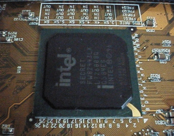
chipsets. To the left is a picture of the LX chipset: |
The LX Chipset, being the first
Pentium II chipset to support SDRAM, supports a maximum of 512MB of SDRAM and a whopping
1GB of EDO if you opt for the slower standard. Fortunately, the LX chipset is able to
improve performance when SDRAM is used with it by requiring special modules with onboard
EEPROM to be used to enable communications between the chipset and the RAM. However, older
modules lacking this EEPROM still work with the chipset almost flawlessly.
| Intel 82440LX Chipset |
| Common Name |
LX AGPSet |
| Chipset Packaging |
Number of chips |
1 (82443LX) |
| Packaging Type |
1 x 492-pin BGA |
| CPU Support |
Number of CPUs |
2 (SMP) |
| AMD CPUs Supported |
N/A |
| Cyrix CPUs Supported |
N/A |
| Intel CPUs Supported |
Pentium II |
| Cache |
Type |
N/A on chip |
| Maximum Supported Size |
N/A on chip |
| Maximum Cacheable DRAM Area |
N/A on chip |
| Memory |
Maximum DRAM Supported |
512MB (SDRAM); 1024MB
(EDO) |
| BEDO DRAM Read Timings (66MHz) |
N/A |
| EDO DRAM Read Timings (66MHz) |
5-2-2-2 |
| FPM DRAM Read Timings (66MHz) |
N/A |
| SDRAM Read Timings (66MHz) |
5-1-1-1 |
| Data Path to Memory |
64-bits |
| ECC Support |
Yes |
| Hard Disk Controller |
Chip |
PIIX4 (82371AB
Controller) |
| Busmastering Support |
Yes |
| UltraDMA Support |
Yes |
| Max. Theoretical Transfer Rate |
PIO Mode 5/DMA Mode 3
(33.3MB/S) |
| PCI Interface |
Supported PCI Bus Speeds |
30, 33 MHz |
| Async. PCI Bus Speed |
No |
| PCI Specification |
2.1 (66 MHz max.) |
| Power Management |
PC97 Compliance |
Yes |
| Suspend to Disk |
Yes |
| HDD Power Down |
Yes |
| Modem Wakeup |
Yes |
| System Suspend |
Yes |
| Video |
AGP Support |
Yes (66/133) |
| Unified Memory Architecture |
No |
| Peripheral Support |
USB Support |
Yes |
| Plug and Play Port |
Yes |
| Write Buffers |
CPU-to-DRAM |
Unknown |
| CPU-to-PCI |
Unknown |
| PCI-to-DRAM |
Unknown |
| Officially Supported Bus Speeds |
60, 66 MHz |
| Unofficially Achieved Bus Speeds |
68, 75, 83.3, ~100 MHz |


4 Comments
View All Comments
vortmax2 - Wednesday, June 25, 2014 - link
The good ole' days when you could put multiple vendor CPUs into the same motherboard. So simple...PentiumGeek - Thursday, September 1, 2016 - link
This motherboard was on my 1st PC. I was very disappointed when faced with the problem that DIMM and SIMM memory can't work in the same time. I used Pentium 100Mhz CPU on this motherboard :)Amadeus777999 - Wednesday, May 9, 2018 - link
Got an ASUS P2L97 board yesterday and I'm reading through this while DoomII is benchmarking. Good times.rogerjowett - Sunday, May 17, 2020 - link
Does n e 1 know where I can find a Voltage Regulation Module please